FEI推出3款透射电镜新产品:Metrios、Talos 和Titan Themis
近日,FEI宣布推出三款专门满足特殊的应用和行业需求的透射电镜(TEM)新品。这三款新产品将为半导体制造和科研提供高效率和有效的特定应用程序。它们是专门用于先进的半导体制造业设的Metrios TEM,为材料和生命科学研究提供高速成像分析的TalosTEM ,以及提供原子量级材料特性研究Titan Themis TEM。
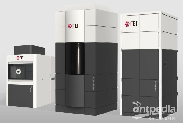
FEI推出三款透射电镜:TalosTEM(左) Titan Themis TEM(中) Metrios TEM(右)
“加上这三个新产品,在过去一年中,我们已经推出了6款TEM新产品,这是前所未有的”。FEI公司执行副总裁兼首席营运官Benjamin Loh说道。“所有6款新产品都是为专门的应用工作流程而设计制造,它们将为科研和工业细分市场的用户提供了信息,如:材料科学,化学,生命科学,半导体制造等领域。我们的目标是完全改变TEM的世界,从而让我们的客户能够改变他们的世界。”
Metrios TEM系统,致力于为需要开发和控制晶片制造工艺的半导体制造商提供快速,精确的测量。透射电镜基本操作和测量程序广泛的自动化,最大限度地减少对操作人员培训的要求。其先进的自动化计量提供比手工操作更高的精度。Metrios? TEM的设计,相比其他电镜,将为客户提供更好的分析通量和较低的成本。
Talos TEM结合高分辨率,高通量的TEM快速成像,以及精确定量的能量色散X-射线(EDX)分析,提供先进的分析性能。新的TEM采用了FEI目前亮度最高的电子源和最新的EDX检测技术,可实现对低浓度和轻元素的高效分析,并拥有FEI独家的3D EDS X射线断层成像技术。在较低的加速电压下,允许使用能量较低的电子束,以减少对样品的损伤。Talos平台是完全数字化的,允许远程操作,并且它可以增加用于特定应用程序的检测器或动态实验的样品架。Talos平台自动化程度高并易于使用,非常适合于个人研究室以及多人操作的实验室。
Titan Themis TEM增强了FEI在原子级成像分析方面的领导地位。研究人员使用高分辨率像差校正TEM来研究大尺寸材料的物理性质以及原子尺度之间的组成和结构的关系。Titan Themis平台可直接测量物理属性,如磁场,纳米尺度,以及下降到原子尺度时的电场。从样品定位到最终数据采集整个流程均实现了自动化,提高结果的重复性和再现性,从而使用户以更少的时间和精力获取更有信心的结论。
FEI launches three new transmission electron microscopy systems: Metrios, Talos and Titan Themis
Julian Heath
Thursday, August 1, 2013
FEI launches three new transmission electron microscopy systems: Metrios, Talos and Titan Themis: The new TEM systems continue FEI’s emphasis on technology and efficient and effective application-specific workflows
FEI has introduced three new transmission electron microscopy systems that tailor the power of TEM to specific application and industry needs. The new systems provide efficient and effective application-specific workflows for semiconductor manufacturing and scientific research. They include the new Metrios TEM for advanced semiconductor manufacturing metrology, Talos TEM that provides high-speed imaging and analysis for materials and life sciences applications, and the Titan Themis TEM for enhanced atomic-scale measurements of material properties.
The Metrios system is the first TEM dedicated to providing the fast, precise measurements that semiconductor manufacturers need to develop and control their wafer fabrication processes. Extensive automation of the basic TEM operation and measurement procedures minimizes requirements for specialized operator training. Its advanced automated metrology delivers greater precision than manual methods. The Metrios TEM is designed to provide customers with improved throughput and lower cost-per-sample than other TEMs.
The Talos TEM (pictured above) combines high-resolution, high-throughput TEM imaging with fast, precise and quantitative energy dispersive X-ray (EDX) analysis to deliver advanced analytical performance. The new TEM is available with FEI’s highest brightness electron source and latest EDX detector technology to provide high-efficiency detection of low concentration and light elements, along with FEI’s 3D EDS tomography. Excellent performance at lower accelerating voltages permits the use of lower beam energies to reduce sample damage on delicate materials. The Talos platform is completely digital, allowing for remote operation, and it also enables the addition of application-specific detectors or sample holders for dynamic experiments. With enhanced automation and ease-of-use, the Talos is especially well-suited for the individual investigator as well as multi-user laboratory environments.
The Titan Themis TEM is for aberration-corrected, atomic-scale imaging and analysis. Researchers use the high resolution of aberration-corrected TEM to understand relationships between a material’s larger-scale physical properties and its atomic-scale composition and structure. The Titan Themis platform enables direct measurements of properties, such as magnetic fields, on the nanometer-scale and electric fields even down to the atomic scale. Automation of the complete TEM workflow, from sample navigation and alignment through final data acquisition, enhances the repeatability and reproducibility of results to enable more confident conclusions with less time and effort.
“With these three systems we have now introduced an unprecedented total of six new TEMs in the past year,” said Benjamin Loh, FEI’s executive vice president and chief operating officer. “All six have been designed and built to provide an application-specific workflow that delivers contextual information of immediate value to users in science and industrial market segments, including: materials science, chemicals, life sciences, and semiconductor manufacturing. Our goal is to completely change the world of TEM so our customers can change their world as well.”
For more information about FEI’s new suite of application-specific TEM workflows, please see http://www.fei.com/tembyfei/, or visit FEI at the Microscopy & Microanalysis Conference, August 4-8, 2013, taking place in Indianapolis, IN, USA.
厂家名称
为全球纳米技术团体提供世界级的显微镜学解决方案 FEI 是一家生产、经营多种科学仪器的业内领先企业。 其产品包括电子和离子束显微镜,以及 可满足多个行业纳米尺度应用的相关产品,这些行业横跨: 工业和理论 材料研究、生命科学、半导体、数据存...