您好,欢迎您查看分析测试百科网,请问有什么帮助您的?

稍后再说 立即咨询
北京欧兰科技发展有限公司
400-6699-117转1000
热门搜索:
分析测试百科网 > MCL > 特种显微镜 > MCL原子力显微镜SPM-M套件

MCL原子力显微镜SPM-M套件

参考报价: 面议 型号: SPM-M
品牌: MCL 产地: 暂无
关注度: 1044 信息完整度:
样本: 典型用户: 暂无
价格范围10万-50万
咨询留言 在线咨询

400-6699-1171000

AI问答
可以做哪些实验,检测什么? 可以用哪些耗材和试剂?

 
SPM-M Kit - build an Akiyama probe or tuning fork AFM with Mad City Labs nanopositioners

  Introduction


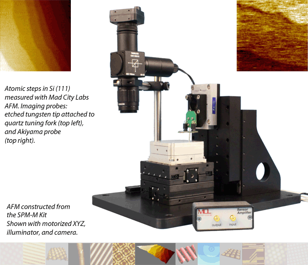
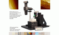
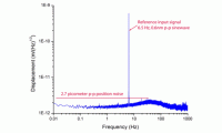
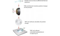
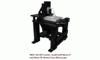
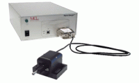
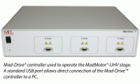
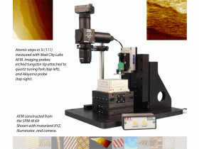
The SPM-M Kit combines the MadPLL® instrument package with Mad City Labs high resolution nanpositioning systems to form a high performance, closed loop, scanning Akiyama probe or tuning fork AFM. The seamless integration of hardware combined with the built-in automated control of MadPLL® means that you can concentrate on getting results, not tweaking parameters.  Applications for the SPM-M Kit include nanoscale characterization and nanoscale fabrication applications such as optical antennas, nano-optics, semiconductors, data storage, and more. The SPM-M Kit is ideal for research and teaching laboratories offering high performance, versatility, simplicity and excellent value.At left: Schematic of a typical AFM instrument based on the SPM-M Kit.The SPM-M Kit includes: MadPLL® Instrument Packagedigital phase lock loop (PLL) controllerprobe mounting boardsfive quartz tuning forksNano-SPM200 nanopositioning stage (XY)Nano-OP30 nanopositioning stage (Z)3 axis closed loop Nano-Drive® controllerZ axis open loop/close loop switch (OCL option)AFMView™ SoftwareAFMView™ TutorialAdapter plate between probe mount board and Nano-OP30Application note: "AFM Kit with manual positioning"Application note: "Tungsten tip etching station"MadPLL® is a powerful instrument package that  allows the user to create an inexpensive, high resolution resonant scanning probe microscope using Mad City Labs nanopositioning systems. The MadPLL® package includes a digital phase lock loop (PLL) controller, software, sensor amplifier board, and resonant probe mounting board. MadPLL® includes five (5) each of the vertical, horizontal, Akiyama, and blank probe boards. In addition, each unit is shipped with five (5) tuning forks. Additional probe boards and tuning forks can be purchased separately.Available options:Double walled isolation enclosureCoaxial illuminatorMotorized or manual Z-axis approachMotorized or manual XY-axisCameraSPM baseplateSPM Etch KitNot included: These items are described in the application note and are listed in the Bill of Materials (BOM)L-BracketFasteners or clampsRecommended additional items:Vibration isolation table


  Absolute Metrology


The SPM-M Kit incorporates the Nano-SPM200 and Nano-OP30 with a three axis Nano-Drive® controller for closed loop nanopositioning in X, Y, and Z.  These systems incoporate Mad City Lab's proprietary PicoQ® sensor technology for closed loop feedback control, offering significant advantages in terms of image quality, accuracy and repeatability over open loop scanners. The sensor signal from all three axes can be read during AFM scans via the analog output signal or USB, thus minimizing the effects of hysteresis, curvilinear motion, and creep that result if data are analyzed using assumed commanded positions. Using position information from closed loop sensors also eliminates the need to scan a calibration grid in XYZ before scanning every sample. Scanning with closed loop nanopositioners saves time  and improves image quality. Closed loop feedback also allows the nanopositioners to move and return to commanded positions with much more reliability than open loop systems, allowing users to return to previously scanned features for further analysis.

For further information about the PicoQ® sensors used in Mad City Labs nanopositioning systems, see the PicoQ® sensor technology page and our Technical Information pages.


  AFM Video Tutorial


Instant AFM - just add science!


 The video at the page linked below illustrates how to use the SPM-M kit along with an Akiyama Probe, manual coarse positioners, and hardware to create a low cost, easy assembly, high resolution AFM.

Mad City Labs AFM Assembly Tutorial - How to Build an "Instant" Atomic Force Microscope


  Image Gallery


Seeing is Believing!


The images below were acquired using similar configurations to the SPM-M Kit.  

Si (111) Atomic Steps    (312pm monatomic layer thickness)    2µm x 2µm    Data taken using MadPLL® with Nano-HS3 3-axis nanopositioning system and etched tungsten tip on a quartz tuning fork.   Si (111) Atomic Steps    (312pm monatomic layer thickness)    1.76µm x 2.02µm    Data taken using MadPLL® with Nano-HS3 3-axis nanopositioning system and Akiyama probe.   Calibration grid    (100nm tall lines, 2µm apart)    10µm x 10µm    Unidirectional scan    Self oscillation mode, constant probe signal    Z force feedback: frequency    Data taken using MadPLL® with Nano-HS3 3-axis nanopositioning system and Akiyama probe.   Calibration grid    (100nm tall pegs, spaced 2µm apart)        10µm x 10µm        Unidirectional scan        Self oscillation mode, constant probe signal        Z force feedback: frequency        Data taken using MadPLL® with Nano-HS3 3-axis nanopositioning system and Akiyama probe.Fly eye    100µm x 100µm    Bidirectional scan    PLL mode, constant probe signal    Z force feedback: frequency    Data taken using MadPLL® with Nano-OP30 nanopositioning system (Z-axis), Nano-OP100 nanopositioning system (XY axes) and Akiyama probe.Human hair    100µm x 100µm    Bidirectional scan    Self oscillation mode, constant probe signal    Z force feedback: frequency    Data taken using MadPLL® with Nano-OP30 nanopositioning system (Z-axis), Nano-OP100 nanopositioning system (XY axes)   and Akiyama probe.PMMA pattern, uncured        10 µm x 10 µm        Bidirectional scan        Self oscillation mode, constant probe signal        Z force feedback: frequency        Data taken using MadPLL® with Nano-OP30 nanopositioning system (Z-axis), Nano-OP100 nanopositioning system (XY axes) and Akiyama probe.Integrated circuit    100 µm x 100 µm    Bidirectional scan     Self oscillation mode, constant probe signal      Z force feedback: frequency      Data taken using MadPLL® with Nano-OP30 nanopositioning system (Z-axis), Nano-OP100 nanopositioning system (XY axes)     and Akiyama probe.Calibration grid    40 µm x 40 µm    Unidirectional scan     Self oscillation mode, constant probe signal      Z force feedback: frequency      Data taken using MadPLL® with Nano-OP30 nanopositioning system (Z-axis), Nano-OP100 nanopositioning system (XY axes)     and Akiyama probe.Calibration grid      (100nm tall, 10µm pitch)      70 µm x 70 µm        Unidirectional scan        PLL mode, constant probe signal        Z force feedback: frequency        Data taken using MadPLL® with Nano-OP30 nanopositioning system (Z-axis), Nano-OP100 nanopositioning system (XY axes)      and Akiyama probe.Etched structures      80 µm x 80 µm    Bidirectional scan     Self oscillation mode, constant probe signal      Z force feedback: frequency      Data taken using MadPLL® with Nano-OP30 nanopositioning system (Z-axis), Nano-OP100 nanopositioning system (XY axes)     and Akiyama probe.


  Tungsten Tip Etching with the SPM Etch Kit


An etched tungsten tip glued to a quartz tuning fork for Atomic Force Microscopy.
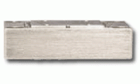
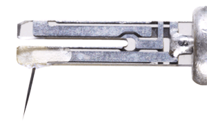
An etched tungsten tip glued to a quartz tuning fork.


 One way to produce sharp probe tips suitable for building an AFM is to electrochemically etch tungsten wire. This method can produce a tip radius of better than 50nm. Post etching techniques can even sharpen the tip down to a <1nm tip radius. These sharp tungsten tips can be mounted to quartz tuning forks for AFM  or for other types of scanning probe microscopy like scanning tunneling microscopy (STM).

There are a variety of methods to choose from to etch the tungsten wire. The single lamella technique is easy to setup and can consistently produce sharp tips. Among the requirements for this process are a metallic ring, a beaker, Potassium Hydroxide (KOH), tungsten wire, and a voltage source. A drop of KOH is added to the metal ring suspended above the beaker, forming a thin film or lamella of KOH inside the metallic ring. The negative terminal of the voltage source is then connected to the suspended metallic ring. This will form the negative electrode. The beaker below the ring is then filled with KOH and the positive terminal of the voltage source is wired intod the KOH solution. This forms the positive electrode. The tungsten wire is then dipped through the center of the lamella and into the KOH in the beaker. The voltage source dis then turned on which begins the etching process. The tungsten is electrochemically etched at the lamella. The etching process automatically stops when the tungsten wire is etched so thin that the portion of wire below the lamella falls off and drops into the beaker. The remaining tungsten wire above the lamella is removed and any remaining KOH or contaminants are rinsed off with distilled water. This leaves a very sharp tip suitable for use in AFM or other types of SPM.

   Mad City Labs provides an SPM Etch Kit along with an application note on etching Tungsten tips to make this easy.


Additional Information

MadPLL® Brochure

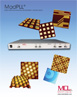
Laser Focus World Article
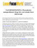

NANOPOSITIONING: Piezo&shy;electric nano&shy;positioners forge low-cost atomic force microscope
AFM Video Tutorial


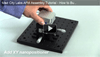
MadPLL® Sensor Probe Board Drawing


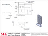
Application Notes:

SPM-004 "Building an AFM with motorized XYZ and camera"
SPM-005 "Building an AFM with manual XY, motorized Z and camera"
SPM-006 "Creating tungsten tips using the Mad City Labs SPM Etch Kit"
SPM-007 "Using shattered silicon as resonant probe tips"

Available upon customer request


Related Products

MCL原子力显微镜SPM-M套件信息由北京欧兰科技发展有限公司为您提供,如您想了解更多关于MCL原子力显微镜SPM-M套件报价、型号、参数等信息,欢迎来电或留言咨询。

注:该产品未在中华人民共和国食品药品监督管理部门申请医疗器械注册和备案,不可用于临床诊断或治疗等相关用途

MCL原子力显微镜SPM-M套件 - 下载资料
MCL原子力显微镜SPM-M套件 - 相关产品
移动版: 资讯 直播 仪器谱

Copyright ©2007-2024 ANTPEDIA, All Rights Reserved

京ICP备07018254号 京公网安备1101085018 电信与信息服务业务经营许可证:京ICP证110310号