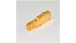


毫米波GAP波导
The gap waveguide is built up of two parts: a structured metal surface and a flat metal surface being placed in close proximity to one another. The structured surface is characterized by pins forming a barrier preventing the electromagnetic waves from propagating in undesired directions, resulting in signal losses as low as for rectangular waveguides.
可以提供26.5~110GHz的GAP转接波导,产品联系:sales@gamtic.com,021-5197 0121.
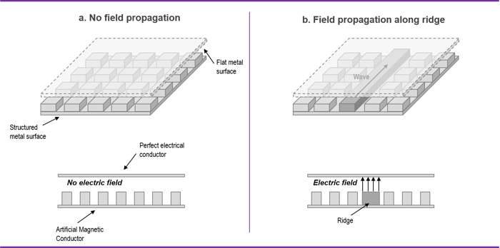
The gap waveguide is built up of two parts: a structured metal surface and a flat metal surface being placed in close proximity to one another (see figure 1). The structured surface is characterized by pins forming a metamaterial surface called an Artificial Magnetic Conductor. The pins create a barrier preventing the electromagnetic waves from propagating in undesired directions. In this way, the pins replace the walls in rectangular waveguides. This is done without requiring a perfectly sealed metallic enclosure. Figure 1a illustrates a scenario with only pins, which shows that no waves can propagate in the structure. However, when ridges are introduced, as shown in figure 1b, waves are allowed to propagate within the pin structure. The waves propagate in the air gap (thereby the name gap waveguide) between the ridges and the top metal surface, resulting in low signal losses. In addition, no metallic contact is required between the two parts, resulting in a much simpler assembly compared to rectangular waveguides that need to be welded or screwed tightly.
 Figure
1. A gap waveguide is built up of a pin structure that prevents the
electromagnetic waves from propagating in undesired directions and
ridges that guide the waves through the structure
Figure
1. A gap waveguide is built up of a pin structure that prevents the
electromagnetic waves from propagating in undesired directions and
ridges that guide the waves through the structure
The open structure of the gap waveguide technology also enables integration of other microwave circuits such as active components. This is done by replacing the flat metal surface by a circuit board making it possible for the gap waveguides to interface directly with the active components.
Comparison with alternative technologies
There are primarily three alternative technologies to gap waveguides: microstrip waveguides, rectangular waveguides and substrate integrated waveguides (SIW) (see Figure 2).
Microstrip waveguides can be produced at a relatively low cost and offer a high design flexibility as they are made using traditional circuit board technology. However, they are lossy at higher frequencies (e.g. at millimeter waves) as the waves travel in a dense medium that absorbs their energy, transforming the signals into heat. When used at frequencies above 20 GHz the losses increases significantly.
Rectangular waveguides have low losses, as the waves travel in a rectangular tube filled with air. However, the technology requires a complex and costly production process using welding or screws. The reason is that the rectangular tubes need to be sealed with a perfect metallic contact to avoid leakage (signal losses).
Substrate integrated waveguides (SIW) are a compromise between microstrip waveguides (in terms of loss) and rectangular waveguides (in terms of cost). As for microstrip waveguides the waves travel in a dense medium (usually a circuit board), but with less energy being absorbed due to the design of the waveguide. However, they still result in losses that limits their use at frequencies above 20 GHz.
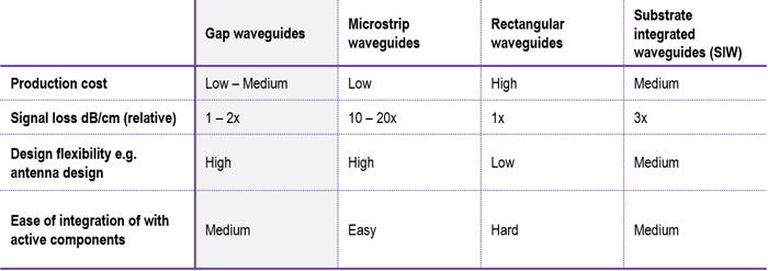 Figure 2. Comparison of gap waveguides and three alternative waveguide technologies