


3D打印毫米波太赫兹无源器件(一)
Bing Zhang,1 Wei Chen,2 Yanjie Wu,3 Kang Ding,4 and Rongqiang Li5
1College of Electronics and Information Engineering, Sichuan University, Chengdu 610064, China
2Department of Electrical and Computer Engineering, Faculty of Engineering, National University of Singapore, Singapore 117583
3School of Physics and Optoelectronic Engineering, Guangdong University of Technology, Guangzhou 510006, China
4National
Key Laboratory on Electromagnetic Environmental Effects and
Electro-Optical Engineering, PLA University of Science and Technology,
Nanjing 210007, China
5School of Electronic Engineering, Chengdu University of Information Technology, Chengdu 610225, China
Correspondence should be addressed to Yanjie Wu
Received 23 March 2017; Revised 10 June 2017; Accepted 19 June 2017; Published 24 July 2017
Academic Editor: Xiulong Bao
Copyright © 2017 Bing Zhang et al. This is an open access article distributed under the Creative Commons Attribution License, which permits unrestricted use, distribution, and reproduction in any medium, provided the original work is properly cited.
Abstract
目前3D打印技术引人注目。 它比传统的制造工艺有一定的优势。 我们从3D打印技术发明的时候开始对3D打印技术进行慢慢的回顾。 该技术也被用于制造毫米波(mmWave)和太赫兹(THz)无源器件。 尽管已经证明了有前途的结果,但是面临的尺寸公差和表面粗糙度等制造公差的改善仍然是一个挑战。 我们提出高阶设备的设计方法来规避尺寸公差,并建议3D打印设备表面粗糙度的具体建模。 相信随着3D打印技术及材料科学和机械工程相关学科的不断完善,3D打印技术将成为毫米波和太赫兹无源器件制造的主流。
广告:伽太科技提供覆盖毫米波太赫兹频段的无源波导器件、天线、毫米波太赫兹有源器件等等,同时提供3D打印机,实现太赫兹透镜3D打印加工、太赫兹波导加工等,具体咨询:伽太科技,sales@gamtic.com,021-5197 0121
The 3D printing technology is catching attention nowadays. It has certain advantages over the traditional fabrication processes. We give a chronical review of the 3D printing technology from the time it was invented. This technology has also been used to fabricate millimeter-wave (mmWave) and terahertz (THz) passive devices. Though promising results have been demonstrated, the challenge lies in the fabrication tolerance improvement such as dimensional tolerance and surface roughness. We propose the design methodology of high order device to circumvent the dimensional tolerance and suggest specific modelling of the surface roughness of 3D printed devices. It is believed that, with the improvement of the 3D printing technology and related subjects in material science and mechanical engineering, the 3D printing technology will become mainstream for mmWave and THz passive device fabrication.
1. Introduction
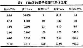
Terahertz (THz) waves, or submillimeter/far-infrared waves, are defined as the electromagnetic (EM) radiation in the frequency from 0.1 to 10 THz. They cover a large portion of the EM spectrum between mid-infrared and microwave bands. This spectral domain has low frequency crystalline lattice vibrations and other intermolecular vibrations in many chemical and biological materials, including explosives, drugs, and other biomolecules. Many polar gases also have the distinctive finger print in the THz spectrum. The absorbed and reflected THz waves of these materials contain information that is not available in other frequency ranges. Hence, the THz is extensively explored for sensing and imaging applications. As a potential modality for sensing and imaging, the THz is considered safe because of its penetration capability through obstacles like paper, textile, ceramic, wood, and leather with negligible attenuation. THz technologies are also used for noninvasive and nondestructive sensing of targets under covers. Recently, THz spectroscopy and imaging of explosive related component have been investigated for defense usage.
Compared with relatively well-developed technologies and widespread applications in microwave, mid-infrared and optical bands, research, design, and technology developments in the THz band are still in infancy. A THz system is built up of various active and passive components. For the antenna and other passive devices, their dimensions are usually proportional to the wavelength. The wavelength of the THz EM waves lies in the range of 3 mm–30 μm, which endows the THz passive devices with very small profile. A small variation of the device dimension might give rise to large shift of the functional band. Consequently, the fabrication of THz antenna and passive devices requires sophisticated process of tight dimensional tolerance. Moreover, the surface roughness is the other equally important decisive factor for the THz antenna and passive devices. Large surface roughness leads to increased insertion loss. Thus, the fabrication process of THz passive device is required to have very smooth surface finishing.
Traditional fabrication methods of THz passive devices are computer numerical control (CNC) machining and electrical discharge machining (EDM) [1, 2]. The CNC process uses computer-controlled precision machine tools to cut the component out of a bulk material, in which the material utilization is low. In addition, the CNC process requires the operator to have sufficient experience and skills, which undoubtedly increases the manpower cost. The EDM etches the workpieces into the desired form by means of electrical discharge, which is usually used for machining super hard materials (such as titanium alloys, carbon steels, and cemented carbides). Its fabrication tolerance is much tighter than the CNC process, but the processing cycle is longer, and the processing cost is higher. From what is mentioned above, high labour cost, long processing cycle, and low material utilization of the traditional process are the main reasons for the high cost of THz passive device. The contradiction between the large demand and the unaffordable cost of THz devices is an urgent problem to be solved in both academia and industry.
In order to meet the requirement of high-precision machining and reduce its manufacturing costs, the 3D printing technology began to be used in THz device fabrication. Most of its applications are seen as the fabrication of passive devices like waveguides, horn antennas, and cavity-based components. The 3D printing technology uses powder or liquid based materials to construct the component layer by layer. Different from traditional subtractive manufacturing (SM) processes, 3D printing is an additive manufacturing (AM) process that is environmentally friendly, of low cost, of low-power consuming, and highly flexible and has a short processing cycle. It has the following advantages:
Efficient material utilization: raw materials that are not sintered or shaped can be used repeatedly; lower energy consumption; less demanding on the operator’s experience and thus lower labour costs; high flexibility: it is capable of realizing complex structure that is impossible to be fabricated by traditional processes, which gives designers more flexibility;
short turn-around time: it eliminates the tool and the mold preparation time; hence the processing cycle is shorter.
In this paper, we will investigate using the 3D printing technology to fabricate THz antennas and passive devices. Firstly, we will review the history of the 3D printing technology. Then 3D printed mmWave and THz passive devices will be introduced. Thirdly, we will elaborate on the key factors for the performance of 3D printed mmWave and THz passive devices which are surface roughness and dimensional tolerance. Finally we will conclude the paper with prospects on the development trend of using the 3D printing technology for mmWave and THz passive device fabrication.
-
项目成果